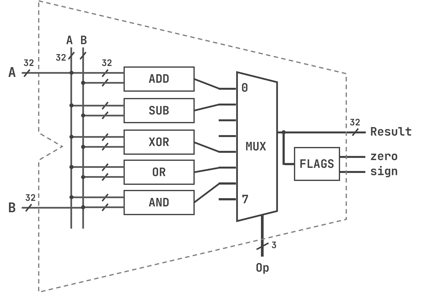
Simplified Logic Diagram of a 32-bit ALU
Back to EECS 31L Index
EECS 31L • Study Notes • Processor Design
Mahmoud Elfar • Spring 2026 • v0.1
v0.1: Initial version
Table of Contents
Loosely speaking, a processor is a piece of hardware that executes instructions. An instruction is a command that tells the hardware to perform a specific operation (ex: add two numbers). But we want our hardware to do more than just addition. As such, the idea of a general-purpose processor emerges: Give me a piece of hardware that can:
Let’s rewrite these requirements in more precise terms:
The program must be stored somewhere. A processor does not know in advance what it will compute. The sequence of operations it should perform must be loaded into memory before execution begins, and the processor must be able to read those operations one at a time.
Execution must be step-by-step and repeatable. The processor reads one instruction, executes it, then moves to the next. State from one step must persist to the next. This requires memory elements — not just combinational logic.
Everything in this note is a direct consequence of these requirements. Some of the historical details were covered in lecture, but they are not part of your exam material, so we won’t cover them here.
Before building a processor, it is important to separate two distinct concepts that are often conflated.
Instruction Set Architecture (ISA) is the contract between software and hardware. It defines:
The ISA says what the processor must do. It says nothing about how.
Microarchitecture is the hardware implementation of an ISA. Two processors can implement the exact same ISA in completely different ways — different numbers of pipeline stages, different cache organizations, different ALU designs — and both will correctly execute the same programs because they both honor the ISA contract.
In this course, the ISA we use in our examples is RISC-V: a modern, open ISA designed for simplicity. The microarchitecture we will implement is the single-cycle processor: every instruction completes in exactly one clock cycle. Later in your career, you will encounter more complex and sophisticated ISAs and microarchitectures, but the basic principles will be the same.
At some point, we will also give an example for how to trace the execution of a program on a processor that uses different ISA and microarchitecture than what you implement in the lab. For this, we will use the Emotion Engine – the processor used in the original PlayStation and PlayStation 2 consoles.
In class, we jumped back and forth between ISA and microarchitecture details. In this note, we will follow a more disciplined approach and start with the microarchitecture first.
A microarchitecture describes the hardware components that implement an ISA. We can divide the components into two categories:
The components within each:
Our focus here is on the datapath building blocks. We will cover how those blocks are interconntected to form the datapath and the controller in later notes.
The Arithmetic Logic Unit (ALU) is the combinational component that performs computations: addition, subtraction, AND, OR, comparison, and so on.
ALU Model:
flags are 1-bit signals that describe properties of the result. The flags used in this course are:
| Flag | Name | Set to 1 when… |
|---|---|---|
zero |
Zero | The result is exactly zero (all bits are 0) |
sign |
Sign | The result is negative (the most significant bit is 1) |
overflow |
Overflow | The result overflows (whether signed or unsigned) |
carry_out |
Carry out | The addition or subtraction produced a carry out of the most significant bit (relevant for unsigned arithmetic) |
Note: Remember that not all carry outs are overflows. In exams, I won’t ask you to compute or model either flags. You have suffered enough through EECS 31.
There can be more flags. In this class, we will focus only on zero and sign – you must know what they mean.
zero is particularly important for branch instructions. For example, beq subtracts two registers and branches if zero is asserted. What is beq, you ask? “Branch if equal”, but that’s a topic for another day.
Here is an example of the logic diagram (simplified for clarity) of a 32-bit ALU.
Simplified Logic Diagram of a 32-bit ALU
From how the multiplexer is wired, we can deduce the ALU control encoding for each operation:
| Operation | ALU control value |
|---|---|
| ADD | 000 (0x0) |
| SUB | 001 (0x1) |
| XOR | 100 (0x4) |
| OR | 101 (0x5) |
| AND | 110 (0x6) |
Some notes:
This is a favorite exam question as it tests your understanding of how the ALU works, as well as your ability to read and interpret logic diagrams and multiplexer control signals.
Purpose:
Construction: You can build a homebrew register file by doing the following:
This is getting out of hand. Just check the logic diagram below. You should be able to build something like this – you studied each component before in EECS 31. It is important to understand how the register file works internally. For 31L exams, you only need to know the input and output ports, the behavior, and how to interpret and select the correct values for W and N.
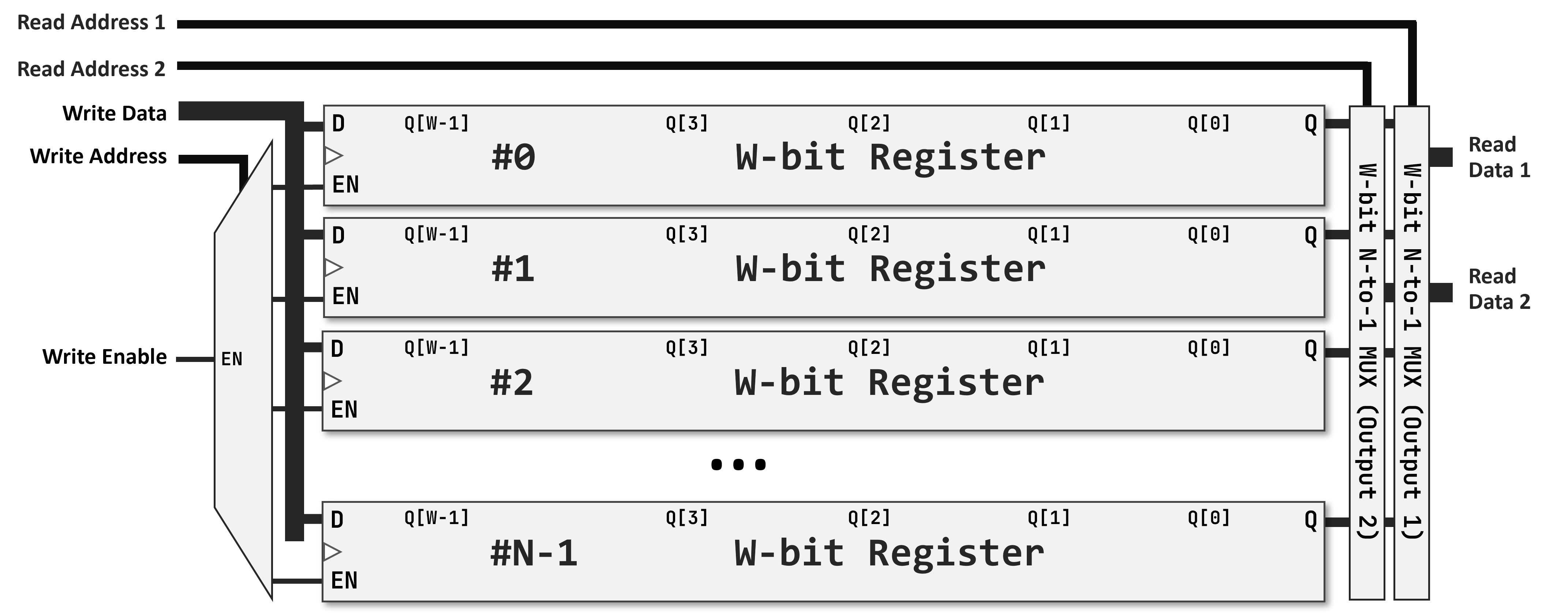
Simplified Logic Diagram of a 32-bit Register File
N×W notation. A register file is described as N×W, or an N W-bit register file, where:
A 32×32 register file, or a 32 32-bit register file, has 32 registers, each is 32 bits wide, with a 5-bit address bus and 32-bit data buses. I guess it is a bad example of naming, but RISC-V’s register file is 32×32.
A better example:
A 64×16 register file has 64 registers, each is 16 bits (2 bytes) wide. Expect the address bus to be 6 bits (log₂64 = 6) and the data buses to be 16 bits wide.
Why two read ports, one write port. Most instructions read two source registers and write one destination register. Having two independent read ports means both operands are available simultaneously in the same cycle — no need to sequence them. One write port is sufficient because an instruction produces at most one result. Adding a second write port would roughly double the decoder and wiring complexity with no benefit for the instruction set we support.
One example of port naming convention is given in the following table. There are many variations, you should get used to encountering a new one, even within the same course.
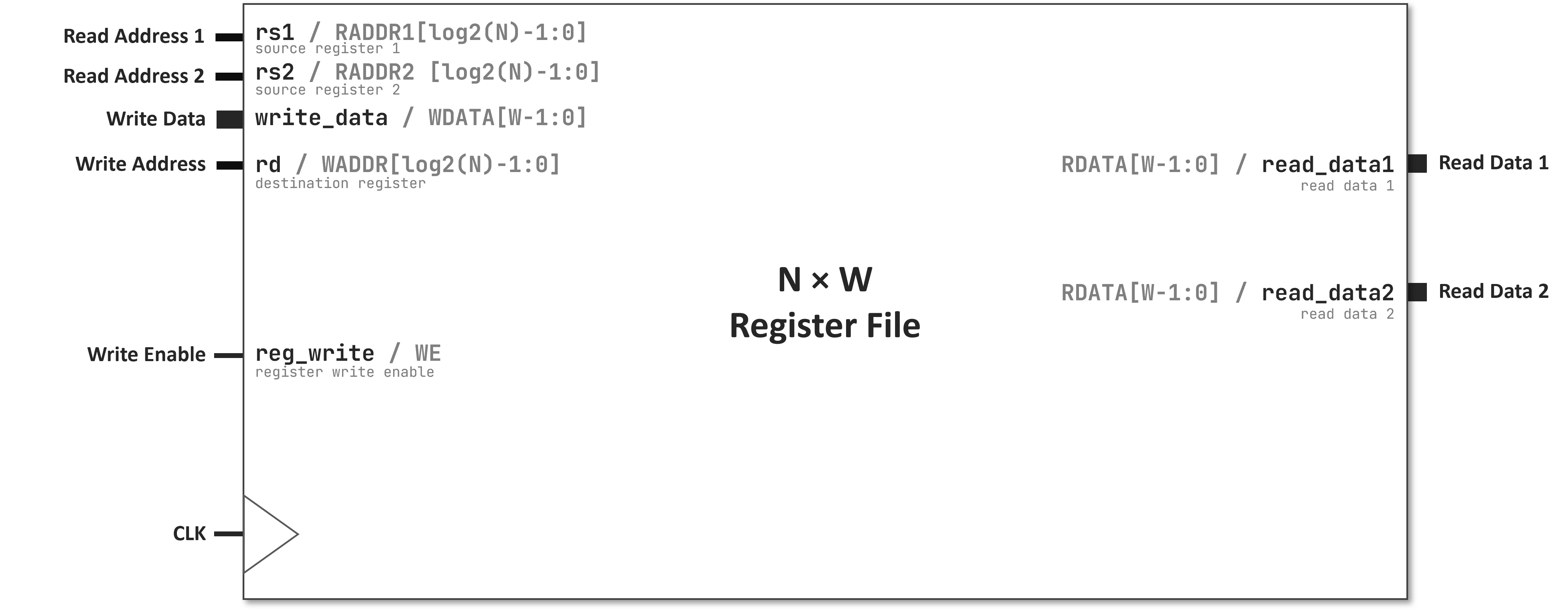
Register File Block Diagram (ports only)
                +-------------+
rg_rd_addr1 ──→ |             | ──→ rg_rd_data1
rg_rd_addr2 ──→ |    Reg      | ──→ rg_rd_data2
rg_wrt_addr ──→ |    File     |
rg_wrt_data ──→ |    32×32    |
rg_wrt_en   ──→ |             |
clk         ──→ |             |
                +-------------+
| Port | Direction | Width | Name in lab |
|---|---|---|---|
| Read address 1 | Input | 5 | rg_rd_addr1 |
| Read address 2 | Input | 5 | rg_rd_addr2 |
| Read data 1 | Output | 32 | rg_rd_data1 |
| Read data 2 | Output | 32 | rg_rd_data2 |
| Write address | Input | 5 | rg_wrt_addr |
| Write data | Input | 32 | rg_wrt_data |
| Write enable | Input | 1 | rg_wrt_en |
Register File Model:
rg_rd_addr1 (read address 1), rg_rd_addr2 (read address 2), rg_wrt_addr (write address), rg_wrt_data (write data), rg_wrt_en (write enable), clkrg_rd_data1 (read data 1), rg_rd_data2 (read data 2)rg_rd_data1 always outputs the value of the register at index rg_rd_addr1 (asynchronous read).rg_rd_data2 always outputs the value of the register at index rg_rd_addr2 (asynchronous read).clk, if rg_wrt_en is asserted, write rg_wrt_data to the register at index rg_wrt_addr (synchronous write).Memory Elements as Register File Variants:
All other memory elements in the processor are variations of the same concept. What varies is the number of registers, the number of read/output buses (1 or 2), and the number of write buses (1 or none).
Purpose:
Construction:
next_pc ──→ [ PC ] ──→ pc_out
clk     ──→ [    ]
Purpose:
Construction:
            +---------+
pc_out ───→ |  IMEM   | ──→ instruction (32 bits)
            |   N×32  |
            |  ROM    |
            +---------+
Purpose:
Construction:
               +-------+
addr       ──→ | DMEM  | ──→ read_data
write_data ──→ |  N×32 |
MemWrite   ──→ |  RAM  |
MemRead    ──→ |       |
clk        ──→ |       |
               +-------+
Every storage element in the processor can be seen as an instance of the same abstraction: a bank of registers, with combinational read and synchronous write. The differences are in scale and access restrictions, not in kind.
| Element | Size | Read ports | Write ports | Type |
|---|---|---|---|---|
| PC | 1×W | 1 | 1 | Register |
| IMEM | N×32 | 1 | 0 | ROM |
| Register File | 32×32 | 2 | 1 | RAM |
| DMEM | N×32 | 1 | 1 | RAM |
In the next two study notes, we will see how do instructions look like, and trace their execution through the datapath.