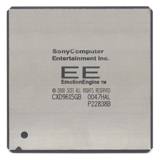
Sony Emotion Engine CPU
Image: Wikimedia Commons, CC BY-SA 3.0.
Back to EECS 31L Index
EECS 31L • Study Notes • Microarchitecture
Mahmoud Elfar • Spring 2026 • v0.1
v0.1: Initial version
Table of Contents
A microarchitecture is the specific design of a processor’s datapath and control unit that implements a given instruction set architecture (ISA). Okay let’s take a step back.
Designing a general-purpose processor involves two parts:
Part 1: An instruction set architecture (ISA), which defines the programmer-visible interface: the instructions, registers, and memory model. An ISA serves two main purposes:
Part 2: A microarchitecture, which defines the actual hardware design that implements the ISA. A microarchitecture specifies how the processor’s datapath and control unit are organized to execute the instructions defined by the ISA. Multiple microarchitectures can implement the same ISA, each with different performance, power, and area characteristics.
Case Study: The Emotion Engine
The Emotion Engine (EE) is a central processing unit (CPU, or microprocessor) developed through collaboration between Sony Computer Entertainment and Toshiba for the PlayStation 2 (PS2) video game console, circa late 1990s. The EE implemented the MIPS R5000 ISA – a 64-bit RISC architecture – as well as some custom extensions developed by Sony.
Sony also developed the microarchitecture of the EE. Game developers who wanted to write games for the PS2 did not need to know anything about the microarchitecture of the EE. Their devkit provided them with the ISA specification, which was all they needed to write software that could run on the PS2. The microarchitecture was Sony’s internal design choice that determined how the EE executed instructions, but it was abstracted away from game developers.
The datapath is the collection of hardware components that perform the actual data processing in a processor. Food processors process food; data processors process data. Okay everyone is tired of those clever analogies:
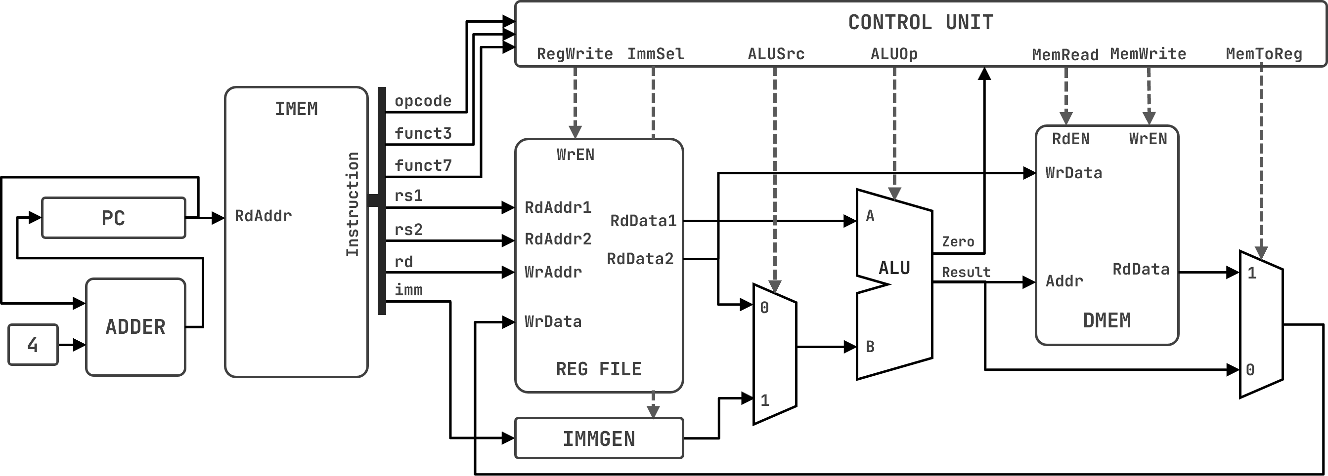
A RISC-V Microarchitecture
Recall the components from study notes 06 – we just added one more component: the Control Unit.
| Component | Type | Description |
|---|---|---|
| Program Counter (PC) |
Sequential | A register that holds the address of the current instruction. Gets updated every clock cycle to point to the next instruction. PC + 4 for the next instruction (since instructions are 4 bytes). |
| Instruction Memory (IMEM) |
Combinational | A read-only memory that stores the program instructions. Takes the PC as input and outputs the instruction at that address. |
| Register File | Sequential | A collection of registers that can be read and written. Has two read ports (for source registers) and one write port (for the destination register). Reads are combinational (outputs change immediately with address changes); writes occur on clock edges. |
| ALU | Combinational | Performs arithmetic and logic operations. Takes two operands and a control signal to determine the operation. Outputs the result and status flags (Zero, Overflow, Carry_Out). |
| Data Memory (DMEM) |
Sequential | A read/write memory for data storage. Takes an address and control signals to read or write data. Reads are combinational; writes occur on clock edges. |
| Immediate Generator (IMMGEN) |
Combinational | Generates immediate values from instruction fields. Takes instruction bits as input and outputs a sign-extended 32-bit immediate value. |
| ALU-Source MUX | Combinational | Selects the second operand for the ALU. Controlled by ALUSrc signal: selects between register data and immediate value. |
| Register-Write-Source MUX | Combinational | Selects the value to write back to the register file. Controlled by MemToReg signal: selects between ALU result and DMEM output. |
| PC Adder | Combinational | Computes the next PC value (PC + 4). Used to advance to the next instruction. |
| Control Unit | Combinational | Generates control signals based on the instruction opcode and function fields. Controls the operation of the datapath components for each instruction type. |
Microarchitectures come in many shapes and forms. In this course, we will focus on a specific microarchitecture for the RISC-V ISA called the “single-cycle datapath”. Understanding this datapath is crucial for grasping more complex designs that you will definitely encounter in the future, whether in your studies or future career.
You should be able to:
FeDEX Store™ is a mnemonic for the four-ish stages of instruction execution: Fetch, Decode, Execute, Store/Writeback.
Fetching an instruction means reading it from the instruction memory.
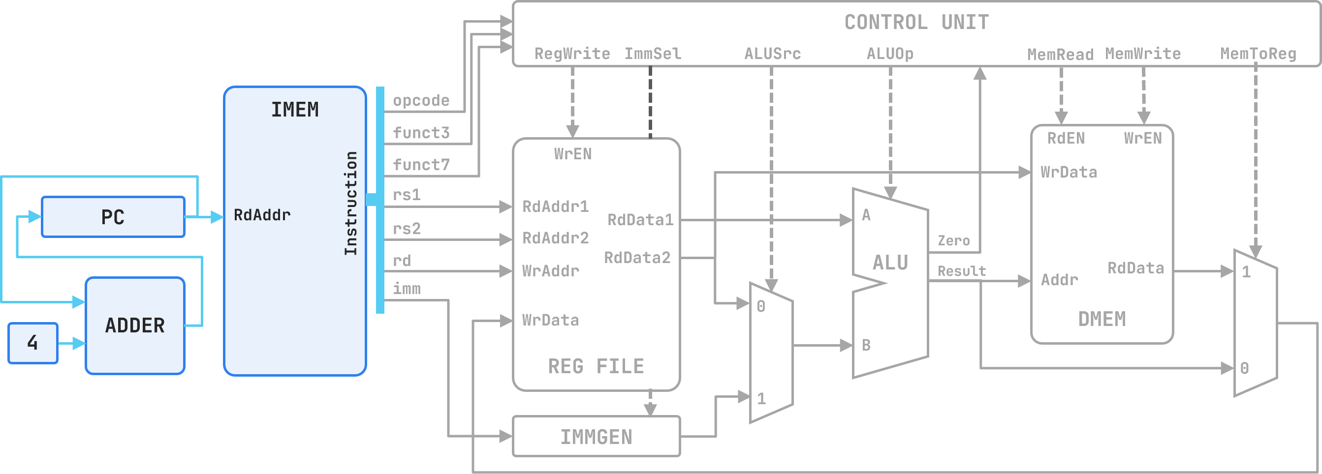
Fetching Stage
Components:
Signals:
pc_out: The current value of the PC, which serves as the address of the instruction to fetch.instruction: The 32-bit instruction word output by IMEM, which will be decoded and executed in subsequent stages.pc_next: The next value of the PC, computed as pc_out + 4.At the end of every cycle the PC must advance. Since every instruction is exactly 4 bytes wide, the next address is always pc_out + 4. A dedicated adder computes this, and the result feeds back into the PC’s write port at the rising clock edge.
Decoding an instruction means splitting the 32-bit word into its named fields, reading the required register values, and generating the control signals that configure the rest of the datapath.
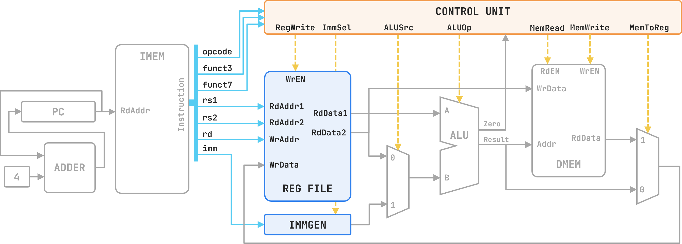
Decode Stage
Components:
rs1 and rs2 as read addresses and asynchronously outputs the values of the two source registers.opcode, funct3, and funct7 and combinationally asserts the control signals that drive every mux select, memory enable, and register write enable in the datapath for the remainder of the cycle.Signals:
instruction[19:15]: the rs1 field — index of source register 1.instruction[24:20]: the rs2 field — index of source register 2.instruction[11:7]: the rd field — index of the destination register (forwarded to later stages).instruction[6:0]: the opcode field — primary input to the Control Unit.instruction[14:12] / instruction[31:25]: the funct3 / funct7 fields — secondary inputs to the Control Unit.rg_rd_data1: the 32-bit value read from register rs1.rg_rd_data2: the 32-bit value read from register rs2.imm_out: the sign-extended 32-bit immediate produced by IMMGEN (unused for R-type instructions).RegWrite, ImmSel, ALUSrc, ALUOp, MemRead, MemWrite, MemToReg: control signals asserted by the Control Unit, which configure the datapath for the specific instruction being executed.Decode is entirely combinational. The register file read and control signal generation both complete within the same clock cycle as fetch. All control signals are stable before the Execute stage begins.
Executing an instruction means performing the required arithmetic or logical computation in the ALU.
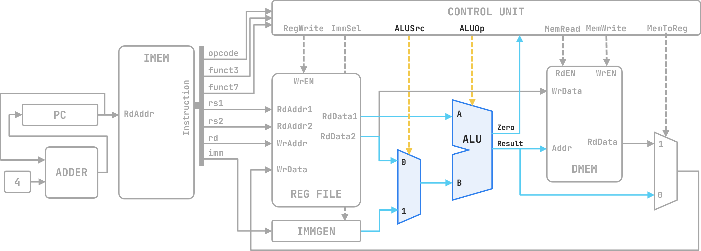
Execute Stage
Components:
ALUSrc = 0, it passes rg_rd_data2 (register operand, used by R-type). When ALUSrc = 1, it passes imm_out (immediate operand, used by I-type and S-type).ALUOp. For arithmetic instructions the result is the computed value; for load/store instructions the result is the effective memory address (rs1 + immediate).Signals:
ALUSrc: control signal (from Control Unit) selecting the ALU’s B input.ALUOp: control signal (from Control Unit) specifying the operation the ALU performs.rg_rd_data1: the A input to the ALU, always sourced from register rs1.alu_b: the selected B input — output of the ALU-source MUX.Result: the 32-bit ALU output. For R-type and I-type arithmetic this is the value to write back; for lw/sw it is the data memory address.Zero: ALU status flag, unused in Labs 3–4 but required for branch resolution in later labs.The Control Unit drives ALUOp directly; no separate ALU controller is shown in this diagram. The same ALU hardware computes the result for R-type operations and the effective address for lw/sw, because both reduce to addition or a specified arithmetic operation at the ALU level.
The memory stage either reads a word from data memory (lw) or writes a word to it (sw). For all other instruction types this stage is idle and passes Result through unchanged.
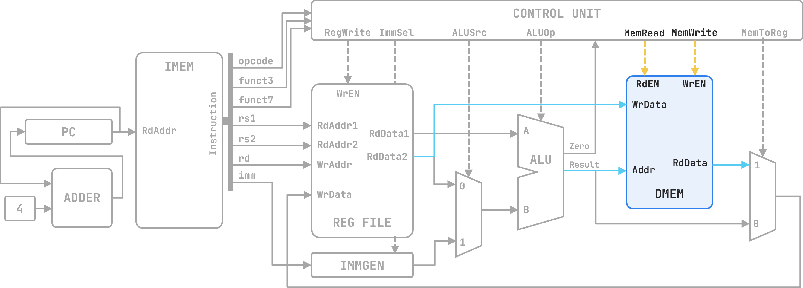
Memory Stage
Components:
Result. On a read (RdEN = 1), the word at that address appears on RdData. On a write (WrEN = 1), rg_rd_data2 is latched at that address on the rising clock edge.Signals:
Result: the memory address, computed in the Execute stage.RdEN: read enable, driven by MemRead from the Control Unit. Asserted for lw.WrEN: write enable, driven by MemWrite from the Control Unit. Asserted for sw.WrData: the data to be written, sourced from rg_rd_data2 (register rs2).RdData: the 32-bit word read from DMEM, forwarded to the Write Back stage.For R-type and I-type arithmetic instructions, the Control Unit deasserts both MemRead and MemWrite, leaving DMEM idle. Result flows directly to the writeback MUX.
Write back selects the result to commit and writes it into the destination register.
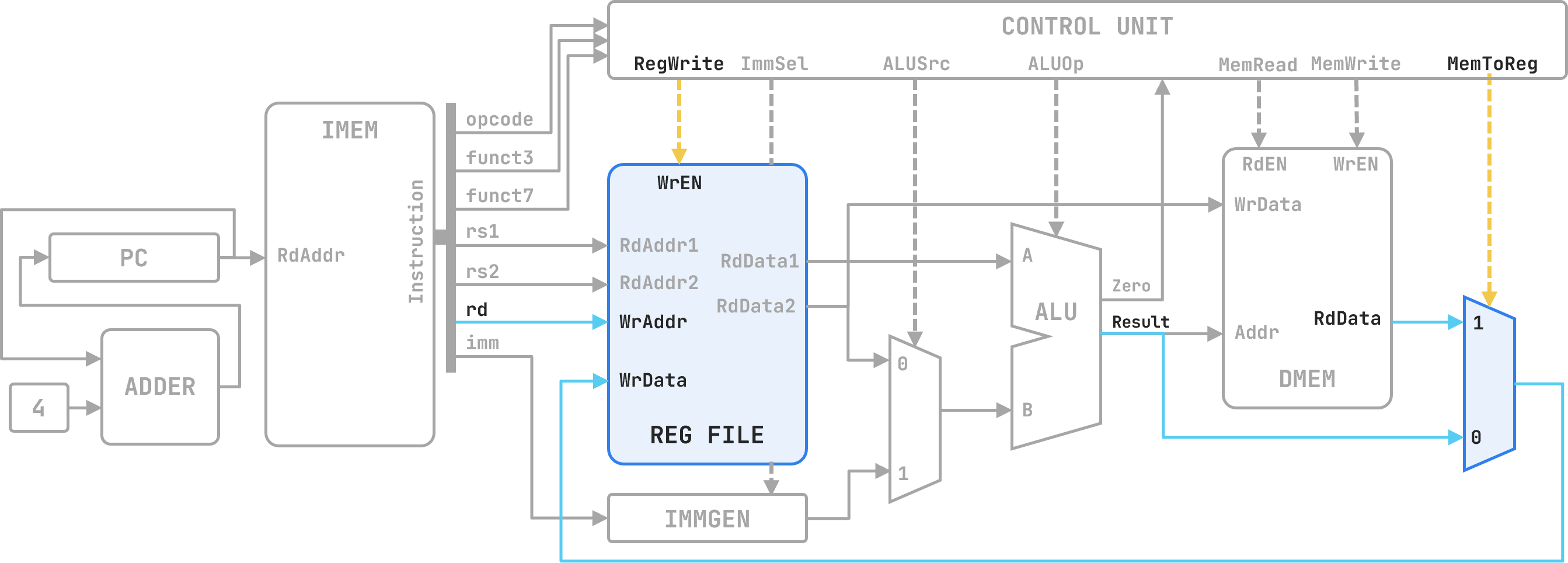
Write Back Stage
Components:
MemToReg = 0, it forwards Result from the ALU (R-type, I-type arithmetic). When MemToReg = 1, it forwards RdData from DMEM (lw).RegWrite = 1, writes the selected value to the register indexed by rd.Signals:
MemToReg: control signal (from Control Unit) selecting the writeback data source.RegWrite: write-enable for the register file, driven by the Control Unit. Asserted for R-type, addi, and lw; deasserted for sw, which has no destination register.WrAddr: the destination register index, taken directly from instruction[11:7] (rd).WrData: the value written into the register file — output of the writeback MUX.Write-back completes at the rising clock edge — the same edge that advances the PC. Every state update in the single-cycle design (PC increment, register write, data memory write) is simultaneous. The next instruction begins fetching with all written values already stable.
Every stage of FeDEX Store is shaped by control signals. The Control Unit is the combinational circuit that generates all of them. It takes the instruction’s opcode, funct3, and funct7 as inputs and asserts the correct combination of control signals as outputs — within the same clock cycle, before the Execute stage begins.
The Control Unit does not process data. It does not add, compare, or store anything. Its only job is to look at what kind of instruction is being executed and configure every mux, every enable line, and every memory port accordingly. It is the part of the microarchitecture that makes the datapath do different things for different instructions.
Inputs to the Control Unit:
opcode — bits [6:0] of the instruction. Identifies the broad instruction category (R-type, I-type arithmetic, I-type load, S-type, etc.).funct3 — bits [14:12]. Distinguishes instructions within the same opcode group (e.g., add vs. and vs. or, all of which share the R-type opcode).funct7 — bits [31:25]. Used in R-type to further distinguish instructions (e.g., add vs. sub).Outputs from the Control Unit:
| Signal | Width | Controls |
|---|---|---|
RegWrite |
1 | Whether to write to the register file at the end of the cycle |
ALUSrc |
1 | Whether the ALU’s B input comes from the register file (0) or the immediate (1) |
ALUOp |
3 | Which operation the ALU performs |
MemRead |
1 | Whether to read from data memory |
MemWrite |
1 | Whether to write to data memory |
MemToReg |
1 | Whether the writeback value comes from the ALU (0) or data memory (1) |
A note on ALUOp: in some textbook designs, the Control Unit outputs a 2-bit ALUOp that feeds a separate ALU Control circuit, which then produces the final 3-bit (or 4-bit) ALU control signal. In the version of the datapath used in this course, ALUOp drives the ALU directly. Either approach is valid; what matters is the final operation the ALU performs.
For the four instruction types we study — R-type, I-type arithmetic (addi, ori, etc.), I-type load (lw), and S-type store (sw) — the Control Unit outputs the following:
| Instruction | RegWrite |
ALUSrc |
ALUOp |
MemRead |
MemWrite |
MemToReg |
|---|---|---|---|---|---|---|
R-type (add, sub, and, or, …) |
1 | 0 | (from funct3/funct7) | 0 | 0 | 0 |
I-type arithmetic (addi, ori, …) |
1 | 1 | (from funct3) | 0 | 0 | 0 |
I-type load (lw) |
1 | 1 | ADD | 1 | 0 | 1 |
S-type store (sw) |
0 | 1 | ADD | 0 | 1 | X |
Notes on reading this table:
X means “don’t care”. For sw, there is no destination register, so MemToReg is irrelevant — RegWrite is 0, so the writeback MUX output is never used.lw, ALUOp is always ADD because the effective address is always rs1 + immediate, regardless of any other field.sw, ALUOp is also ADD for the same reason.ALUOp is determined by funct3 (and funct7 for R-type). The Control Unit passes enough information to the ALU to let it determine the exact operation.ALUSrc = 0 for R-type only. Every other instruction type in this table uses an immediate, so ALUSrc = 1.Given an instruction, you should be able to state the value of every control signal. The process is:
Example: add x5, x1, x2
This is R-type. From the table:
RegWrite = 1 — we write the result to x5.ALUSrc = 0 — the ALU’s B input is x2 (from the register file), not an immediate.ALUOp = ADD (determined by funct3=000, funct7=0000000).MemRead = 0, MemWrite = 0 — no memory access.MemToReg = 0 — write the ALU result, not a memory read, to the register file.Example: lw x7, 36(x2)
This is I-type load. From the table:
RegWrite = 1 — we write the loaded word to x7.ALUSrc = 1 — the ALU computes the address using the immediate (36), not a second register.ALUOp = ADD — address = x2 + 36.MemRead = 1 — we read from data memory at the computed address.MemWrite = 0 — no write.MemToReg = 1 — write the data memory output (the loaded word) to the register file, not the ALU result.Example: sw x5, 12(x11)
This is S-type. From the table:
RegWrite = 0 — there is no destination register; nothing is written to the register file.ALUSrc = 1 — the ALU computes the address using the immediate (12).ALUOp = ADD — address = x11 + 12.MemRead = 0 — no read.MemWrite = 1 — write x5 to data memory at the computed address.MemToReg = X — irrelevant; RegWrite = 0 ensures the register file is never written.To be continued…